Semiconductor testing is a fundamental process to ensure reliability, performance, and compliance with specifications. Through advanced testing systems, it is possible to identify non-compliant devices, optimize production yield, and minimize the risk of failures in critical applications.
The importance of semiconductor testing
What is the purpose of semiconductor testing?
Semiconductor testing aims to identify and eliminate defective devices, with a particular focus on outliers (erratic deviations) from expected values. This process ensures the reliability and quality of microchips by detecting and removing components that exhibit anomalies.
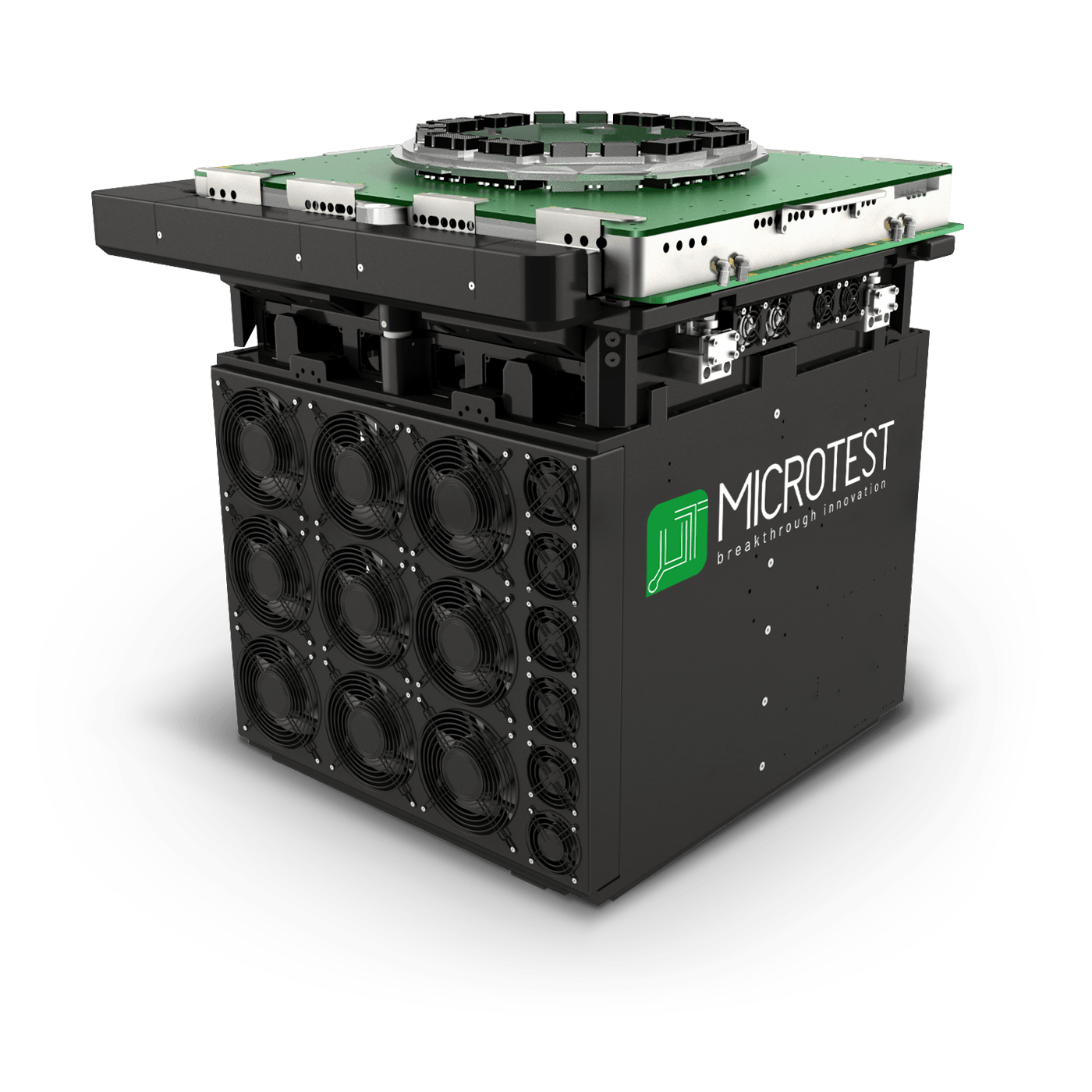
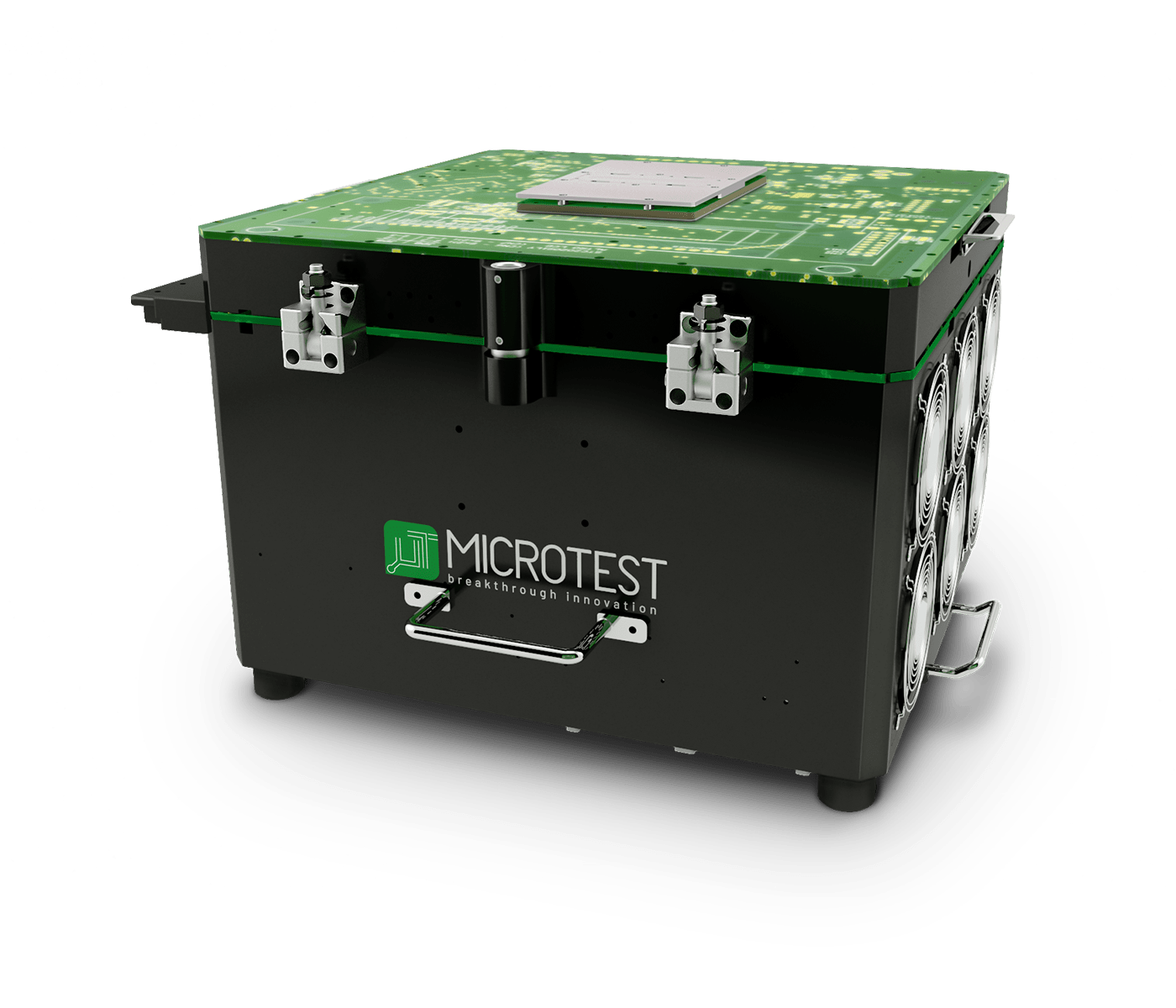
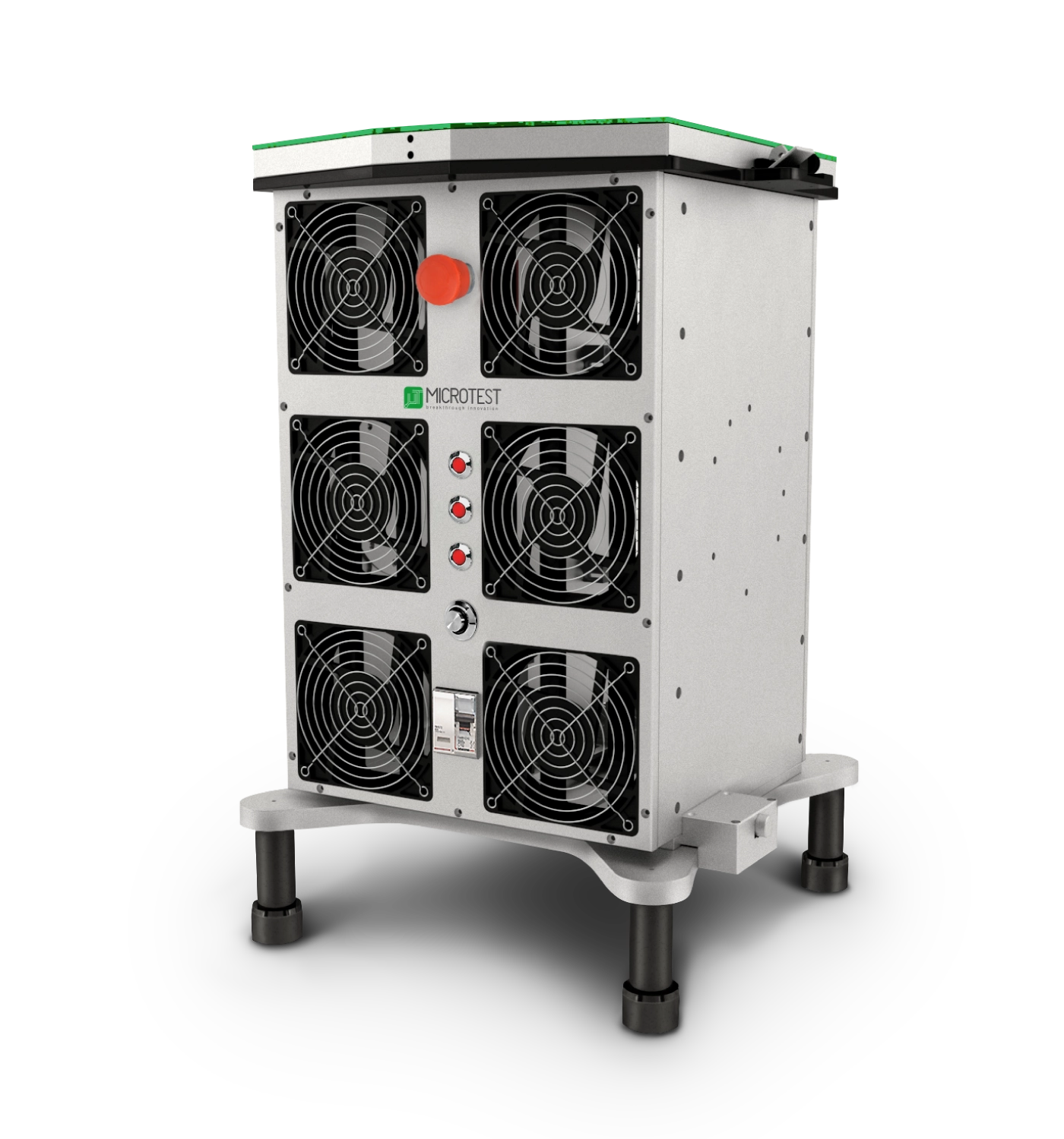
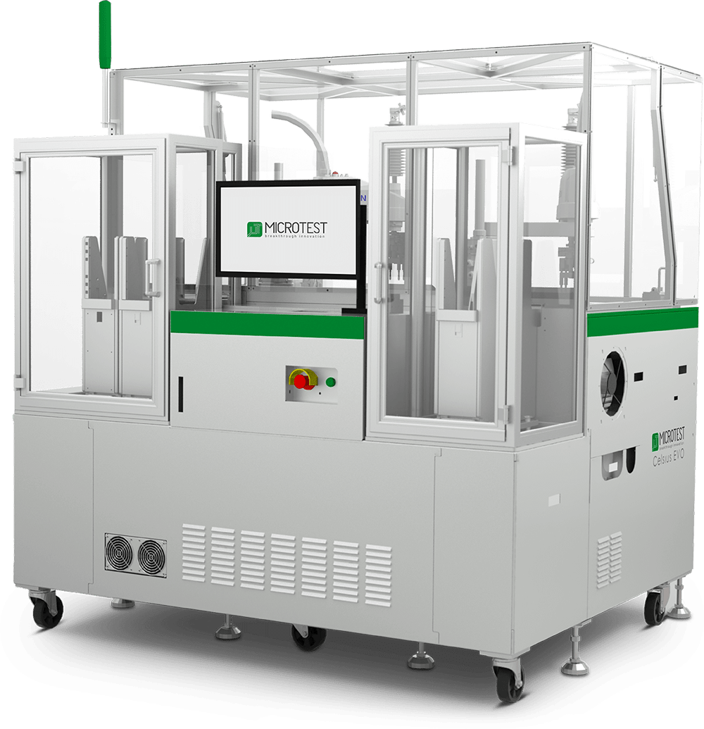
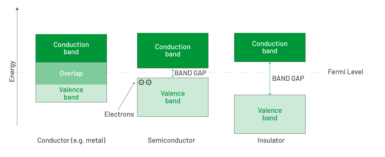
Semiconductor testing is performed using dedicated semiconductor test systems, commonly known as ATE (Automated Test Equipment) or simply Testers.
Microtest stands out as one of the leading manufacturers of semiconductor test systems, offering a comprehensive portfolio of innovative solutions. This includes ATE machines, MEMS (micro-electro-mechanical systems) testing solutions, Mixed Signals, Power Device Testing, Handlers, and equipment for processes such as Burn-In and HTOL (High Temperature Operating Life).
The importance of compliance in semiconductor testing
The test program is developed based on the datasheet, which defines the electrical specifications and functionalities of the device, to verify its compliance with the stated parameters.
This process applies to various contexts and is particularly crucial for safety critical devices.
However, an initial compliant test may not detect certain phenomena, such as infant mortality. To enhance device quality, additional testing phases, such as Burn-in, may be introduced.
Leveraging its expertise and a comprehensive range of automated test equipment for semiconductors, Microtest implements advanced methodologies to significantly improve the quality and reliability of tested devices.
Test Program
The TP (Test Program) must meet the following requirements:
The test program must ensure 100% coverage of the device’s functionalities, verifying every aspect comprehensively and exhaustively.
The test program must be optimized to minimize test duration, enhancing operational efficiency. Thanks to the high multisite parallelism typical of Microtest solutions, it is possible to achieve fast and accurate results. Key factors to consider include:
-

Power and Energy Consumption
Reducing the ATE’s energy consumption to ensure sustainability and efficiency.
-

Footprint
Minimizing equipment size, making it an ideal solution for space-constrained environments.
To ensure compliance, the test program must be designed to verify the device without compromising its integrity, preventing EOS (Electrical Over Stress), which means, e.g, damage caused by excessive voltage or current.
Testing procedures must adhere to industry regulations and quality certifications, such as IATF 16949 for the automotive sector, along with other relevant industry-specific certifications.
So far, we have emphasized the importance of the Test Program in ensuring a device’s quality. However, to achieve even higher levels of quality in semiconductors, additional verification steps can be introduced:
- Outlier Removal: eliminating devices that deviate from the expected parameter distribution.
- Burn-In: a crucial process to mitigate the risk of infant mortality in devices. For more details on Burn-In, visit the following link
Types of Semiconductor Testing
Semiconductor testing is divided into two main types:
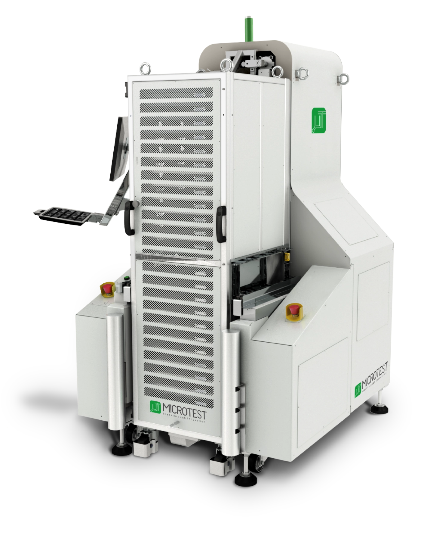
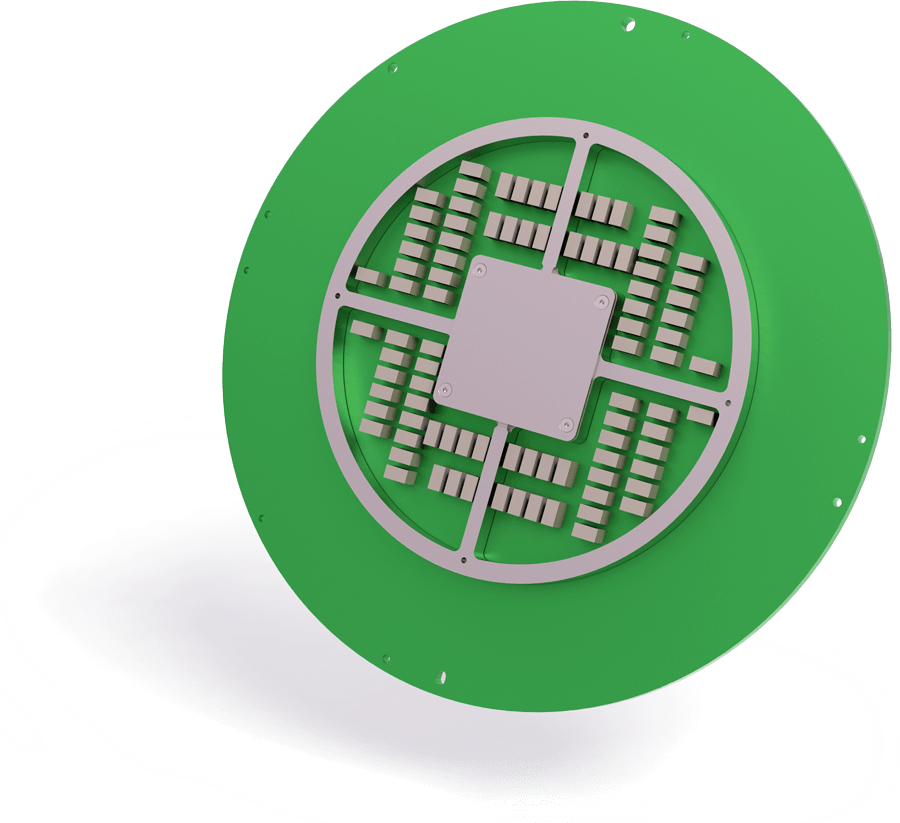
WS (Wafer Sorting) is a test performed directly on the silicon wafer, which typically has a diameter of 6″, 8″, or 12″ and can contain thousands of devices. To perform this test, a semiconductor probe station (prober) is used. The prober handles the wafer and houses the probe card, which enables contact with the DUT (Device Under Test). Microtest stands among the most recognized wafer testing companies in Europe.
The Final Test (FT) is performed directly on the discrete device (packaged chip) using specialized equipment such as handlers, which manage the movement and temperature conditioning of the Device Under Test (DUT). Depending on the specific project requirements, it is possible to conduct only the final test, without the need for Wafer Sorting.
With over 25 years of experience in the industry and specialized expertise in ATE design and manufacturing as well as testing services, Microtest ensures maximum reliability across both semiconductor testing services (WS + FT).
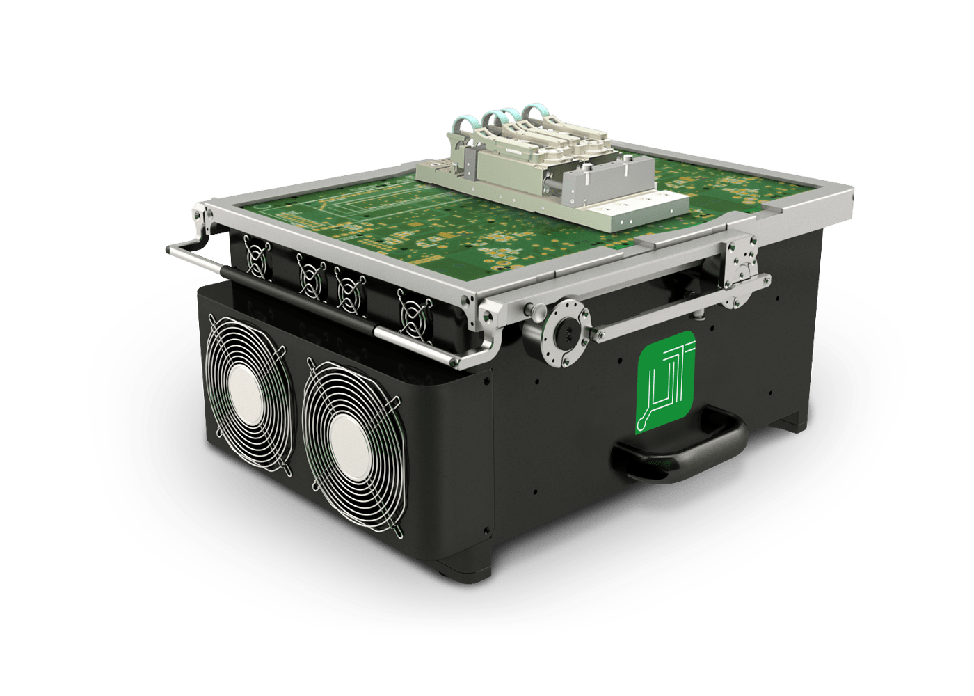
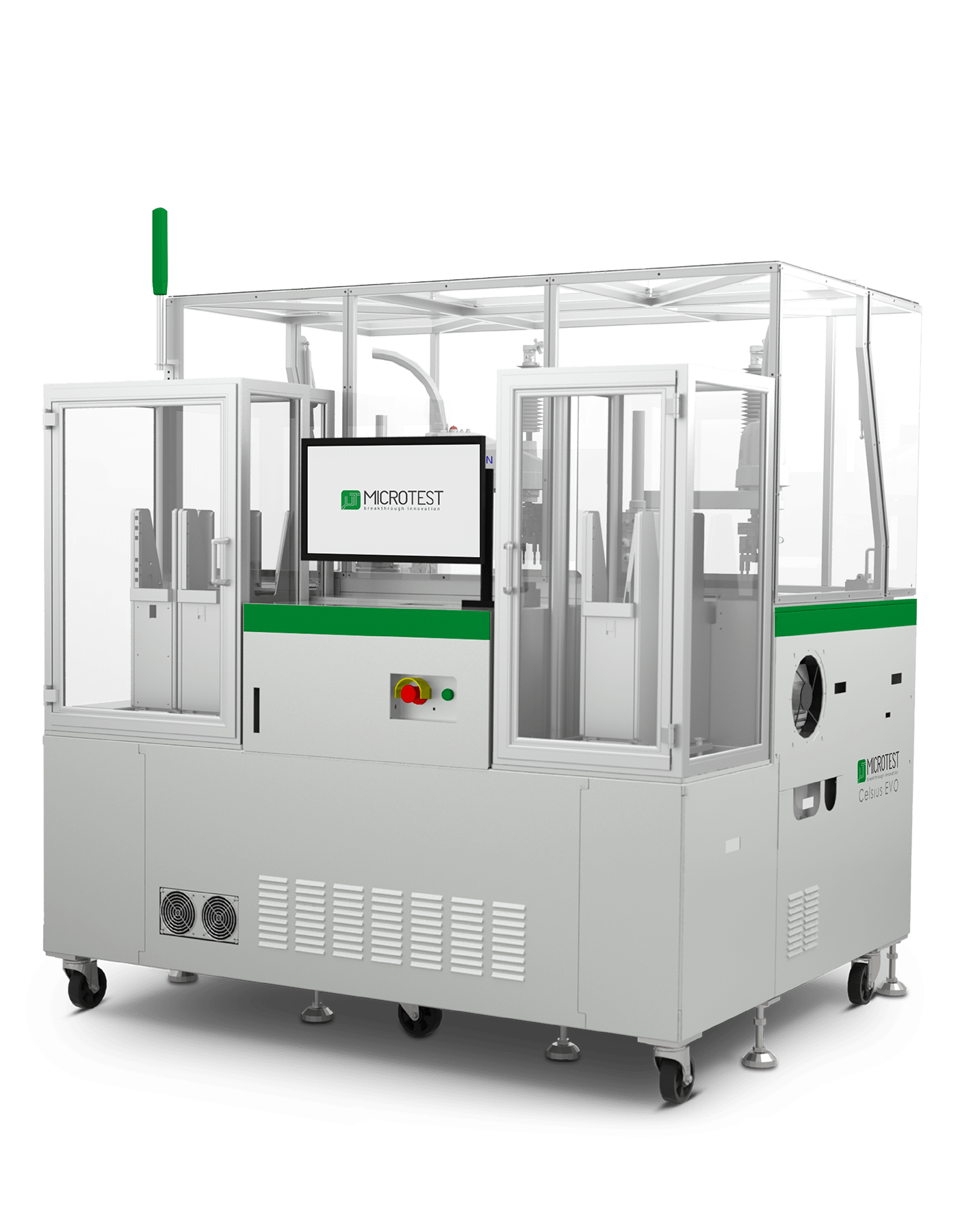
Automated Test Equipment
To carry out effective semiconductor testing, the use of Automated Test Equipment (ATE) is essential. Microtest offers the following devices and services:

Microchip Assembly and Testing
To describe the Microchip Assembly and Testing process, we start with the silicon wafer, where the DIEs are, the first step in the semiconductor manufacturing chain.
Once the DIEs are singulated (sawing), the defective ones are discarded while the functional ones are mounted on package, with a process known as Microchip Assembly, or more commonly, Assembly.
What we do: Innovation
The Microtest Group operates within the semiconductor ecosystem, providing test systems (ATE, Automatic Test Equipment), test services (OSAT, Outsourced Semiconductor Assembly and Test), and high-quality ASIC design.
Serving the automotive, industrial, energy, sensor, and medical sectors, Microtest is the ideal partner for high-tech companies looking to maximize performance, enhance parallelism, and implement state-of-the-art automation solutions, optimizing business operations while reducing testing costs.
With over 25 years of experience, Microtest is headquartered in Italy and is recognized for its steady commitment to innovation, quality, and service excellence.
Applications Across Different Sectors
Semiconductor testing is essential in all industries where ensuring the reliable performance of chips is critical, such as consumer electronics, automotive, aerospace & defense, medical and many more. The semiconductor reliability test is particularly crucial in safety-critical applications, such as healthcare, aerospace, and other high-reliability fields, where fault tolerance and precision are paramount.

The characterization process is performed on a newly manufactured device to verify its performance against the datasheet specifications. If discrepancies are identified, a redesign may be required to ensure compliance. Characterization is conducted exclusively in the initial phase and is aimed at optimizing production yield.
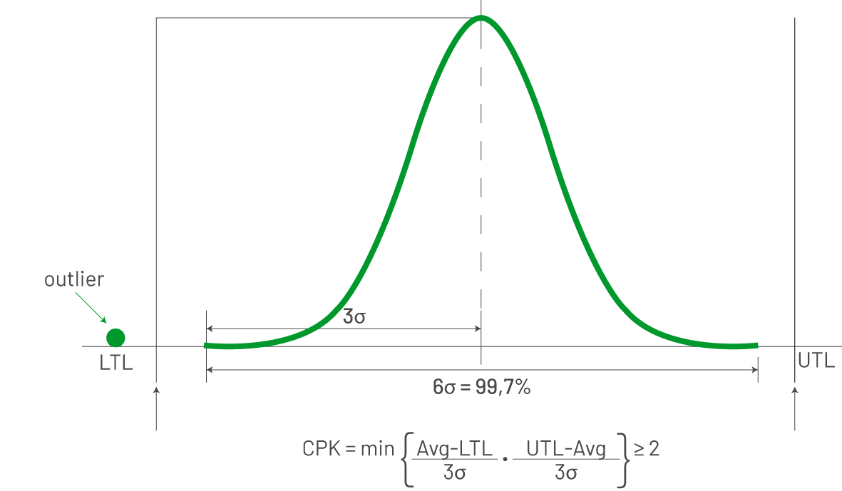
Among the various statistical analyses performed on the data collected from a given number of devices, the CPK for each tested parameter is particularly noteworthy. This index represents the minimum value between two ratios. The difference between the mean value and the lower limit, divided by three times sigma, and the difference between the upper limit and the mean value, also divided by three times sigma. In this context, three times sigma represents half of the Gaussian distribution.
Difference Between Characterization and Production Testing
Characterization
In this phase, device parameter distributions are analyzed, typically represented by a Gaussian curve. The goal is to verify the device’s performance to ensure compliance with the specifications stated in the datasheet. For example, characterization may include testing the device’s functionality under different temperatures or different supply voltages to assess its reliability across varying conditions.
Production Testing
The purpose of production testing is to identify and discard defective units from the production line. This phase relies on test results obtained during characterization. The primary objective is to optimize the process by minimizing test time while maintaining high quality and compliance. Production testing is designed to be efficient and scalable, ensuring that all manufactured devices meet the required specifications.
The Semiconductor Reliability Test is a reliability assessment performed only at the beginning of a device’s lifecycle. These tests, whether conducted fully or partially, help enhance device quality, especially when performed under stress conditions. For example, in the ESD (Electrostatic Discharge) test, the device is subjected to a high-voltage electrical discharge to verify that it maintains full functionality. Among key reliability tests:
- HTOL (High Temperature Operating Lifetime)
- HTRB (High-Temperature Reverse Bias)
- ESD (Electrostatic Discharge)
- LU (Latch-Up)
- PP (Pressure POT)
The Semiconductor System Level Test (SLT) evaluates the device on a test board, simulating its behavior in the final application. For this reason, SLT is considered an application-oriented test, as it verifies the device’s operational performance within an environment that closely mirrors its actual use case.
MOSFETs (Metal Oxide Semiconductor Field Effect Transistor) are a type of transistor that controls current flow based on the voltage applied between two terminals. This enables them to function as both amplifiers and switches in electronic circuits.
When referring to SiC (Silicon Carbide) and GaN (Gallium Nitride) MOSFETs, which belong to the Wide Bandgap (WBG) materials category, we are discussing devices capable of handling high currents and energy levels at extremely high voltages. These high-voltage devices require voltage tests ranging from a few hundred to several thousand volts, with current levels varying from tens to thousands of amperes.
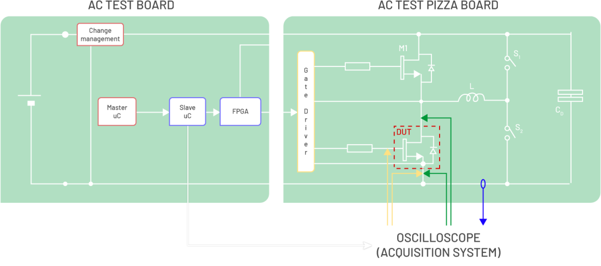
In the High Voltage Stress Test category, which includes Dynamic and AC tests and is also performed on SiC and GaN devices, there are:
- double pulse test
- reverse recovery test
- short circuit test
- UIS (unclamped inductive switching test)
Within a Test Program, certain tests have a high screening potential, including the following:
- The first test in the Test Program is the semiconductor continuity test, which verifies the electrical continuity of the circuit. These are screening tests typically performed by leveraging the presence of ESD DIODES on the DUT PINS. Through the semiconductor continuity test, the entire measurement setup is simultaneously validated (DUT + SOCKET + DIB + ATE). The continuity test serves as a coverage verification: if the test is successfully passed, it confirms that the measurement setup, even if complex, has been correctly configured and is fully operational.
- Maximum or Absolute Ratings: this test category is based on the device’s datasheet and verifies its maximum tolerance limits. At the end of the test, the DUT must remain undamaged, demonstrating its ability to withstand the specified stress levels.
- Power Consumption Test: this test measures the device’s current consumption across its power supply inputs. If the measured values fall outside the expected range, typically being too high, the component is considered defective and discarded.
- LEAKAGE (leakage test semiconductor): the term “leakage” refers to undesired current loss. This test is fundamental for all high-resistance pins in integrated circuits. By applying voltage to a pin, the test assesses the insulation quality of the device.
After these screening tests, the actual coverage measurements for the device begin, ensuring full verification of its specifications.
Advantages of Microtest Solutions
Microtest is committed to integrating sustainability into every aspect of its operations, from manufacturing processes to the products and offered services. This approach also benefits customers, who can take advantage of highly energy-efficient solutions. But what makes Microtest products stand out in terms of sustainability, productivity, and efficiency? The answer lies in the combination of multiple attributes, which are the intrinsic characteristics that define their performance. Let’s take a closer look at these key features:
DIMENSIONS
Microtest products are among the most compact on the market. This, combined with a minimal (or even zero) footprint, enables high performance in terms of space savings.
HIGH PARALLELISM
High parallelism has always been a defining feature of Microtest products, designed with this capability at their core. A high-parallelism testing system enables faster time-to-market, improved efficiency, and lower operational costs, making it essential in high-production sectors such as semiconductors. In testing systems, high parallelism refers to the ability to simultaneously execute a large number of tests across multiple units or devices, optimizing both time and resource utilization. Ultimately, sustainability is at the heart of this approach. Beyond its positive impact on the ecosystem, sustainability also translates into significant cost savings.
POWER CONSUMPTION
Power consumption in an ATE (Automatic Test Equipment) is a critical parameter, as it directly impacts efficiency, operational costs, and reliability. An optimized energy consumption reduces system heating, enhancing measurement stability and extending the lifespan of hardware components.
TIME-TO-MARKET
Time-To-Market (TTM) is a key factor in ATE systems, as it determines how quickly a new product can be tested and launched. A reduced TTM allows companies to stay ahead of the competition, maximize profits, and respond swiftly to market demand. Optimizing testing processes with high-parallelism solutions and low power consumption helps shorten validation times without compromising quality, accelerating the entire development cycle.
Discover Kronos, the Software Toolset by Microtest, which generates faster, more efficient Test Programs by automatically translating test descriptions from natural language into code.
Microtest Specialized Services: ASIC Design and Testing Services
In addition to providing products, Microtest offers a range of highly specialized services, divided into two main areas: ASIC Design and Testing Services.
ASIC DESIGN
Our core activities focus on the design and development of complex electronic systems and integrated circuits (ICs). We support the entire development process, from system-level design or application-specific requirements to final implementation and validation.
Key Expertise:
- Analog mixed-signal design
- Power management
- Low-power design
- Engineering support for product development
Microtest Offers Three Levels of ASIC Design Services:
- Outsourced Design Service
- IP Blocks Design & Portfolio
- Full ASIC/ASSP Design (Application Specific Integrated Circuit / Application Specific Standard Parts)
In addition to these services, Microtest also supports customers in specialized activities, such as Design for Testability, helping to define the most efficient test model and optimizing testing time and process efficiency.
Testing Services
Among semiconductor testing services, Microtest provides:
- Development and production of test solutions
- Wafer (WS – Wafer Sorting) and package (FT – Final Test) characterization
- Qualification and reliability testing
- Production testing on wafer (WS) and package (FT)
- Failure & Technology Analysis (FTA)
Microtest is the ideal partner for a turnkey service across the entire semiconductor supply chain, offering a single point of contact for streamlined operations. With deep expertise, Microtest supports customers from ASIC design to product commercialization and beyond, providing advanced failure analysis services.
Many testing activities are managed in-house within strategically located Microtest test houses. For processes such as silicon manufacturing and assembly (OSAT – Outsourced Semiconductor Assembly and Test), Microtest collaborates with a network of qualified partners.
Types of Semiconductor Tests Offered:
Microtest provides a wide range of semiconductor tests, including:
- Power Consumption Measurement
- Absolute Rating Verification
- Scan Test
- Functional Testing
Tests can be performed at multiple temperature levels, tailored to customer specifications.
Contact us to learn how we can support your project!
Get in touch
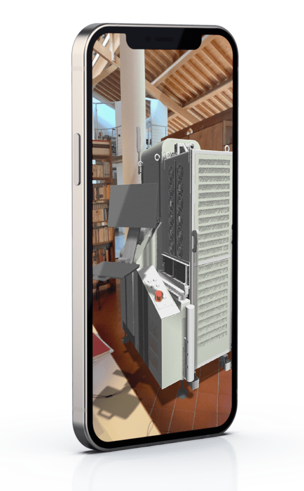
Everytime and everywhere by your side
The App virtually places the 3D model of the selected Microtest ATE on a flat surface in order to highlight the compact form ensuring a visualization as realistic as possible of how the machinery will look like in the workplace.

Glossary
-
Chip
A chip is a miniaturized electronic component made from semiconductor material, also known as a microchip or integrated circuit (IC). It integrates circuits on a small DIE. A chip can contain discrete components or complex functions, such as processors or sensors. When undergoing testing, it is referred to as a DUT (Device Under Test). As the key element of modern electronics, the chip is essential for a wide range of technological devices.
-
CPK
The CPK (Process Capability Index) measures the margin relative to the closest limit of the Gaussian distribution, using a standard tolerance coefficient, typically set to 2. Characterization is crucial for identifying parameters with a low CPK, as these may lead to yield loss during production.
The CPK consists of Capability (CP= the difference between specification limits divided by six times sigma. A CP greater than 2 indicates a robust process), K: a centering factor.