In the semiconductor ecosystem, the semiconductor Burn-In process is one of the most delicate and sensitive procedures as it helps prevent inherent defects, commonly recognized in electronics and described by the so-called bathtub curve. This curve illustrates the defect rate throughout the product lifecycle of a component. Given the natural occurrence of infant mortality failure of components, the Burn-In test procedure aims to identify those components that exhibit early failure and must therefore be intercepted and discarded. If these defective components are released into the market, they could cause severe malfunctions and potentially harm people or property.
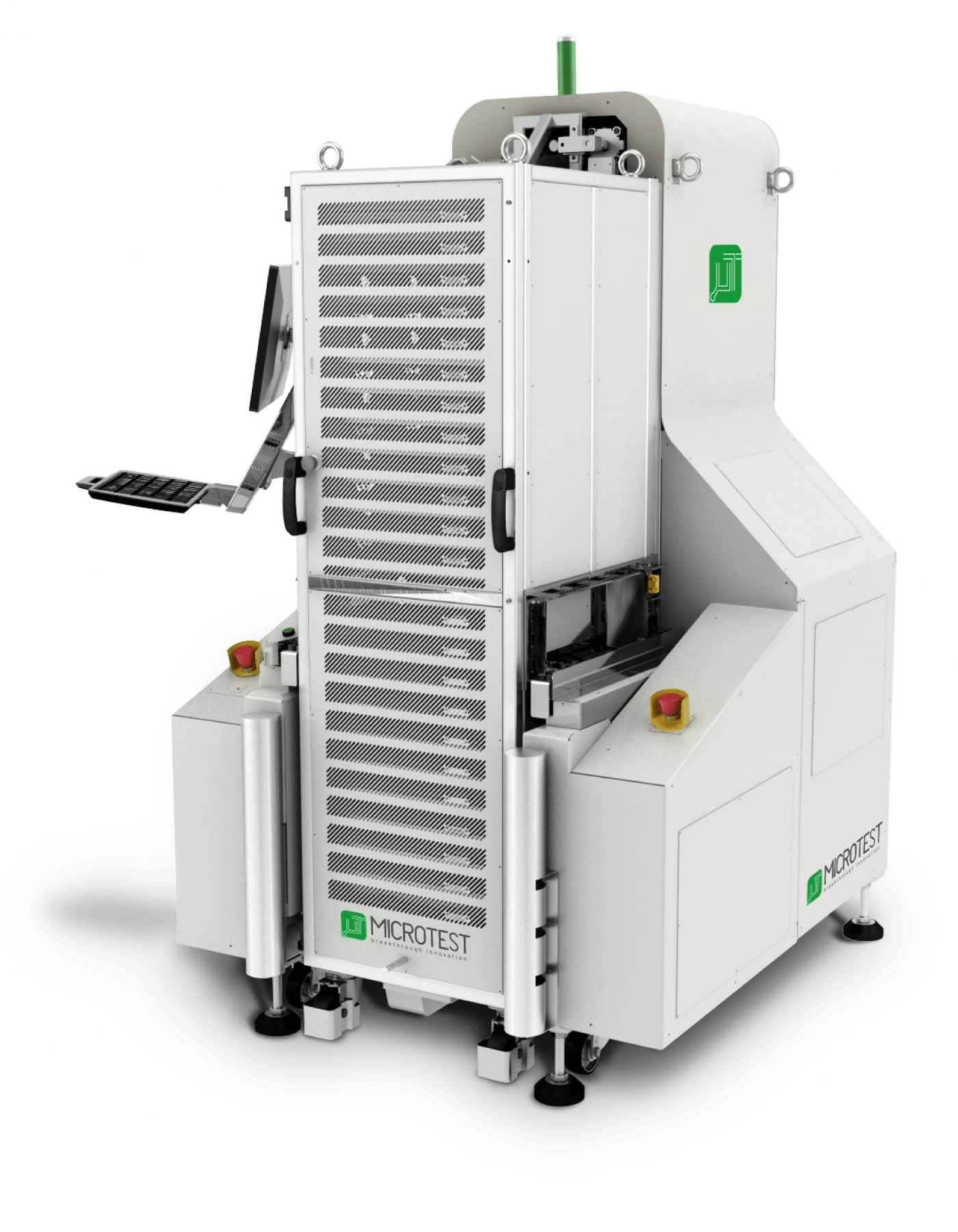
The Burn-In system developed by Microtest is revolutionary because it is ovenless, introducing disruptive innovation and significant improvements over traditional systems used for microcontrollers.
The Burn-In test system acts as a life accelerator (to detect early semiconductor failures). Infant mortality failure is a high-risk factor because failing to detect potential early failures can severely impact the reputation of device manufacturers. Conversely, a robustly tested system enhances the perceived quality of the product due to its long-term reliability. Quality comes at a cost, such as when the Burn-In test procedure must be performed on 100% of the units.
The challenges of traditional Burn-In testing
Based on Arrhenius’ chemical reaction theory, we know that aging is regulated by two parameters: temperature and electrical stress. Traditional systems opted for an approach using a large thermal chamber where all components were simultaneously placed, along with the necessary hardware to ensure functionality. Essentially, a board, sockets, and a thermal chamber with large footprint were used, causing the aging of the entire board (including components not intended for testing), leading to significant thermal inefficiency due to high heat dispersion.
This inefficiency remains a problem for those not using an ovenless burn-in system.
Thus, two inefficiencies are avoided thanks to ovenless Burn-In procedure:
- thermal dispersion (because the process affects everything in the thermal chamber)
- the requirement for large spaces due to the chamber’s size
Moreover, traditional systems are unsustainable in terms of environmental impact, as they struggle to maintain uniform temperature across all levels and positions, leading to reduced energy efficiency and further affecting environmental sustainability.
Microtest’s
Innovative approach
Microtest’s Burn-In System is revolutionary due to its ovenless technology.
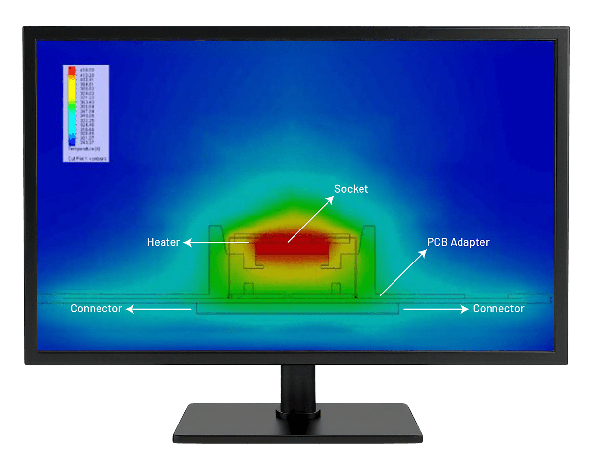
This means each semiconductor undergoes a localized and customized test. A patented localized heater, which emits heat through a coil, is positioned in the socket housing, ensuring the heater is close to the semiconductor and conducts heat through its pins.
Microtest is able to monitor the temperature of each individual DUT (Device Under Test). This is advantageous not only in terms of efficiency but also precision, as the chip itself may generate heat during operation.
Microtest can monitor temperature accuracy with a maximum deviation of +/- 1 degree centigrade (HIGH ACCURACY of DUT temperature (+/-1°C)), as only the individual piece is heated, not the entire thermal chamber.
Microtest’s Burn-In equipment includes:
- BIS (Burn-In System)
- RACK
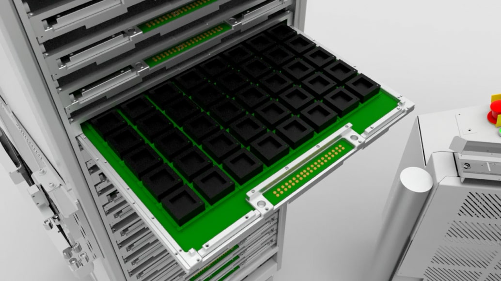
- BID (24 slot inside the RACK) each capable of housing up to 120 devices.
Each batch can accommodate up to 120 devices * 24 slots, significantly optimizing the process time.
BID models with 80 and 60 slots are also available.
Microtest’s clients optimize their production by using multiple racks in their ‘Smart Factory’ setup. While one rack is in the BIS, operators efficiently prepare the next, ensuring the BIS operates continuously without downtime.

From the bottom up:
0. BIS
All contacts are “POGO PINS,” used to connect two objects requiring electrical contact. POGO PINS offer numerous connection cycles before needing replacement, making them durable.
1. BID
BID (Burn-In Driver) Creates stimuli and collects information. It is general purpose. In the traditional approach, it was external, but with Microtest’s innovative patented method, the heating is localized so the driver is not affected (i.e., it doesn’t heat up).
2. BIHU
Positioned above the BID/driver, BIHU (Burn-In Heater UNIT), it is customized by Microtest for the socket and device, designed according to client specifications.
3. SOCKET
Soldered above the BIHU, allowing the device to be tested and removed without damage.
4. DUT (DEVICE UNDER TESTING)
Placed at the top
Talking about Efficiency and Green Technology, the heating and therefore energy consumption are low cost, because only the component is heated, with high-density population volumes under test. Additionally, different tests can be managed simultaneously in different slots.
Key Features of Microtest’s Ovenless Burn-In system
Using Microtest’s Ovenless Burn-In System offers numerous benefits related to Energy Efficiency and cost savings. It is also sustainable since, in case of component failure, only the BIHU (the single housing) is damaged, not the entire board, keeping management and maintenance costs low and providing power saving.
Benefits of adopting Microtest’s Ovenless Burn-In system
Burn-in semiconductor testing is a critical activity to identify devices prone to early failures, or “infant mortality failure”, which are devices with a short lifespan. Isolating defective devices ensures higher quality. This activity can be seen as costly for companies that need to test their devices, but it is vital to avoid inherent costs from potential early failures of devices released to the market.
Regarding Burn-In semiconductor processes, Microtest collaborates with companies aiming to maintain high-quality standards while maintaining a cost reduction policy, enhancing process efficiency (Increased Production Efficiency), and focusing on sustainability (Enhanced Sustainability).
Microtest offers both complete burn-in systems and burn-in services for specific production batches. Clients can rely on Microtest as the ideal partner to support this activity with products or services tailored to their needs.
For Microtest’s catalog product, the Ovenless Burn-In & HTOL solution here are additional benefits:
USER FRIENDLY
The simple yet comprehensive interface allows the operator to interact with the machine easily and intuitively.
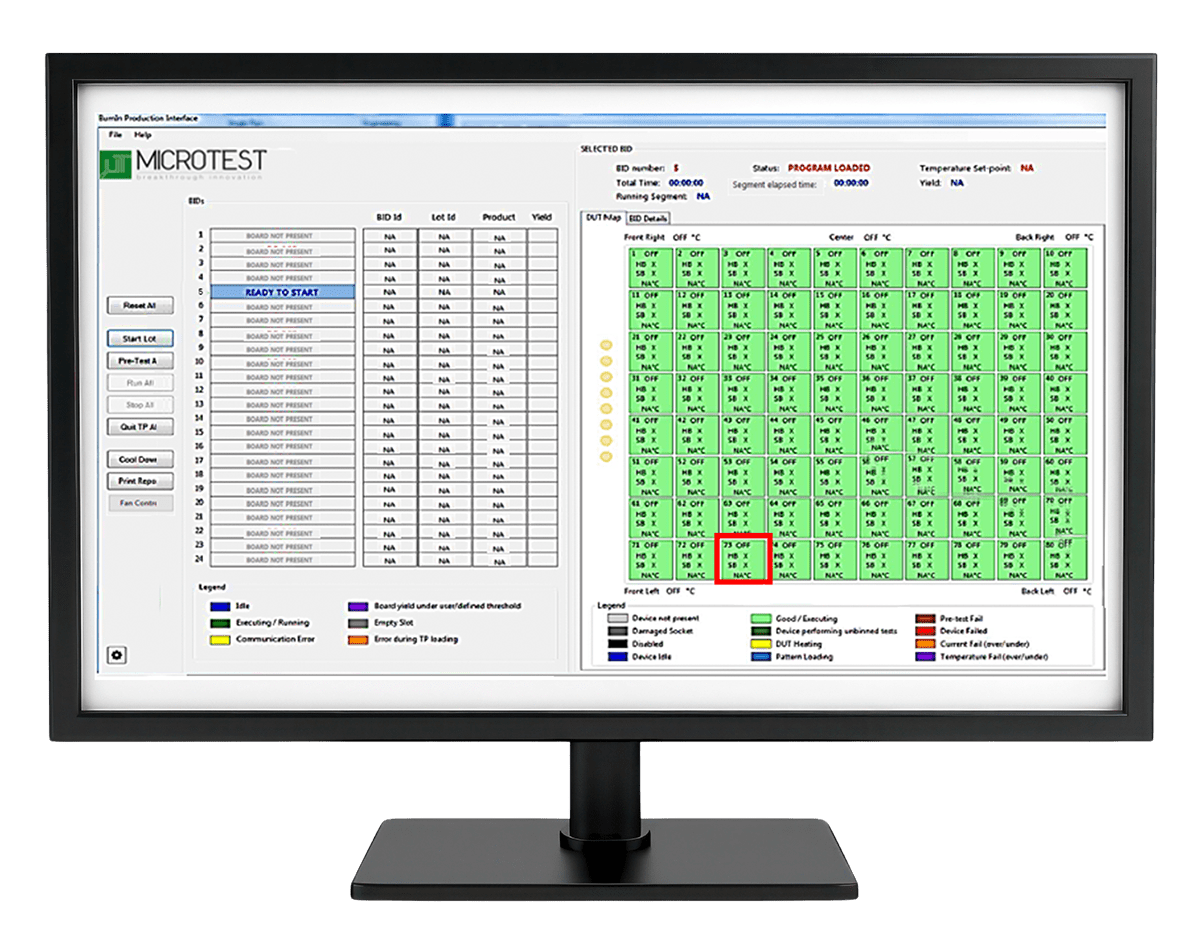
The interface allows the user to view the HB (Hardware Bin) SB (Software Bin) of each DUT. In addition, it is possible to visualize the temperature of each DUT.
It’s possible to view the temperature in the specific areas of the board.
When the Test is running, and after clicking on a specific slot the user can view the corresponding DUTs status.
The interface allows the user to view the HB (Hardware Bin) SB (Software Bin) of each DUT. In addition, it is possible to visualize the temperature of each DUT.
FLEXIBILITY
The rack can be partially filled with different products.
ELECTRONIC PERFORMANCES
The features of Microtest’s Ovenless Burn-In System allow the drivers to be close to the devices under test (DUTs), preventing voltage drops in device power supplies. It also offers numerous digital channels and analog resources to stimulate DUTs compared to the traditional approach.
Applications
Across Industries
The semiconductor burn-in process is applicable across the entire semiconductor industry, ensuring companies can maintain high-quality standards for their products, whether for consumer electronics or more sophisticated applications such as automotive, aerospace, defense, and medical sectors.
The need for burn-in testing varies depending on whether it involves safety-critical applications, where the correct device operation is crucial for safety and human life.
 Automotive
  Consumer
  Medical
  Mems
Mems  Defence
  Space
Space  Industrial
  Power
Power Get in touch
Everytime and everywhere by your side
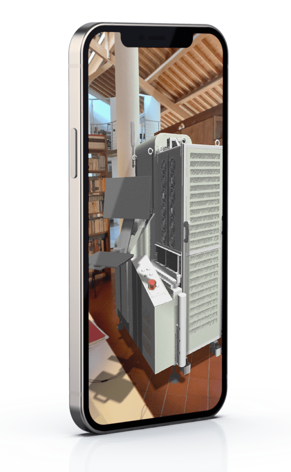
The App virtually places the 3D model of the selected Microtest ATE on a flat surface in order to highlight the compact form ensuring a visualization as realistic as possible of how the machinery will look like in the workplace.